-
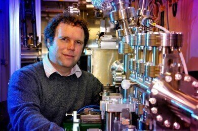
 Armin Wagner, Principle Beamline Scientist
 -
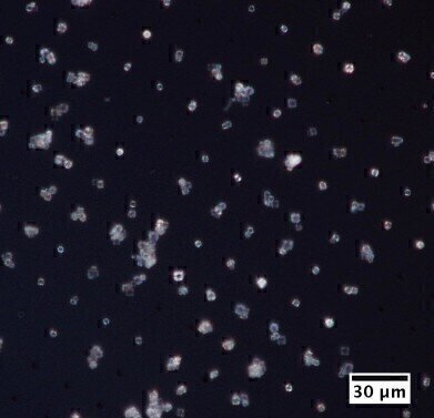
 ChipHolder: The microcrystals arrange themselves in an array of holes at 20 micrometres distance. Image courtesy of DESY
 -
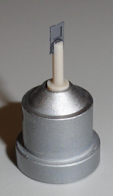
 About 20 000 microcrystals fit on the two square millimetres silicon chip which is fixed on a magnetic mount. Image courtesy of DESY
News & Views
Diamond Helps with Studies of the Tiniest Microcrystals
Oct 23 2015
Unpicking the mysteries of microcrystals can be a huge challenge for scientists. But a European team led by scientists from DESY – a German national research centre composed of a series of particle accelerators – have now used Diamond to develop a new type of sample holder in which several thousand microcrystals can be positioned on a single silicon chip at the same time and then be examined by crystallographic methods. Scientists crystallise biological molecules such as proteins or viruses, and then use X-ray crystallography to visualise their atomic structure allowing us to understand how they function. Many of these structures are essential to understanding biological processes and developing new types of drugs. However, obtaining crystals can be difficult and time consuming.
At Diamond, crystals are exposed to intense light in the form of X-rays; this results in the diffraction patterns from which the atomic structure is determined. Recent developments in X-ray sources with increasing brilliance, such as Diamond, DESY’s PETRA III, or the new generation of free electron lasers (FELs), have opened the door to examining ever smaller crystals. These microcrystals are considerably easier to “grow”, but because of their small size they call for new approaches in preparing specimens.
Researchers from DESY in Germany, the Paul Scherrer Institute in Switzerland and Diamond Light Source in the UK have developed a new type of sample holder for ‘serial protein crystallography’. The holder consists of a single crystal of silicon with a regular array of pores. As the tiny crystals fall into the pores, the holder allows them to be positioned with great precision, while at the same time producing virtually no disruptive signal of its own during the X-ray diffraction experiment, something that is unavoidable using conventional methods. About 20,000 microcrystals fit on the two square millimetre silicon chip, all of which could be scanned in less than three minutes at a source such as the LCLS in California, making it an extremely effective mechanism for crystallography experiments.
The team used Diamond’s I24 beamline to test the effectiveness of the new chip. Armin Wagner, one of the paper’s authors and principal beamline scientist for Diamond’s Long-wavelength MX beamline, comments: “Chips provide an exciting new way for sample mounting, both at sources such as Diamond and at free electron lasers, and could help address many of the challenges associated with sample mounting in microcrystallography. This is a great example of how synchrotrons are assisting with technical advances for the new FELs, where experimental time is extremely precious. We’ll be refining the chip technique further with experiments at LCLS in July using crystals supplied by the Division of Structural Biology (STRUBI) at the University of Oxford.”
The chip can be used at microfocus beamlines of synchrotron light sources such as Diamond, as well as with X-ray free electron lasers such as the LCLS in Stanford and the forthcoming European XFEL in Hamburg. In contrast to the methods typically used so far, such as liquid jets, in which microcrystals are surrounded by a liquid or a gel and then analysed using X-rays, the new sample holder positions the crystals in small holes in a membrane made from a single silicon crystal, just ten micrometres thick, which can then be scanned by an X-ray beam. This technique ensures that the crystals can be accurately located.
“Our new sample holder allows us to characterise tiny microcrystals with a unique level of efficiency,” explains Alke Meents, the scientist at DESY who is in charge of the work. Philip Roedig, a scientist at DESY and the principal author of the study, continues: “You can think of the chip as being like a sieve. The silicon membrane consists of a matrix of many tiny holes which are slightly smaller than the crystals themselves. In order to prepare the specimen, a drop of the mother solution containing the microcrystals is placed on top of the chip, and then the solution is drawn off from below. The crystals are left sticking in the holes, like in a sieve, and can be scanned by the X-ray beam, crystal by crystal.”
Research published in the journal Scientific Reports 5, Article number 10451
Digital Edition
LMUK 49.7 Nov 2024
November 2024
News - Research & Events News - News & Views Articles - They’re burning the labs... Spotlight Features - Incubators, Freezers & Cooling Equipment - Pumps, Valves & Liquid Hand...
View all digital editions
Events
Nov 18 2024 Shanghai, China
Nov 20 2024 Karachi, Pakistan
Nov 27 2024 Istanbul, Turkey
Jan 22 2025 Tokyo, Japan
Jan 22 2025 Birmingham, UK


.jpg)


